
The Advanced Packaging Revolution: Glass Core Substrates vs. Organic Substrates
Walk into any discussion about next-generation AI accelerators or high-performance computing today and you will hear something that would have sounded odd a decade ago: people are arguing about substrates. Not just about die size or node technology, but about what sits under the silicon – glass core substrate or traditional organic substrate. That debate captures a quiet revolution in advanced packaging and heterogeneous integration, as the industry tries to stretch system-level performance without relying solely on transistor scaling.
This is not just a materials story. It is about power delivery, signal integrity, mechanical stability, thermal paths, and how all of those interact in a world where chips become systems and packages become platforms. Glass core substrates promise new capabilities in flatness, line width, and dimensional stability; organic substrates offer mature, cost-effective, and well-understood solutions. The revolutionary part is that package substrate choice now determines what is possible at the system level. That makes understanding the trade-offs between glass and organic cores essential for anyone involved in advanced packaging or heterogeneous integration.
Why Substrates Suddenly Matter So Much
For years, the substrate under a chip was seen as relatively mundane. It routed signals from the die to the board, handled power and ground planes, and provided mechanical support. As long as it met basic electrical and reliability requirements, it did not draw much attention. What really mattered were the transistors on the die and the interconnect inside it.
That mental model breaks down once packages begin hosting:
- Multiple large dies in 2.5D or 3D configurations.
- High-bandwidth memory stacks surrounding logic.
- Chiplets and heterogeneous dies from different nodes and vendors.
Now the substrate has to behave like a high-performance printed circuit board with micron-scale line/space, low loss, dense power delivery networks, and tight mechanical tolerances. It becomes an active participant in performance, not just a passive platform. As interposer sizes grow and bump pitches shrink, the mechanical limits and wiring density of traditional organic substrates are pushed to their limits. That is where glass core substrates enter the conversation.
Organic Substrates: The Established Workhorse
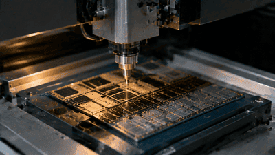
Organic substrates – typically built from resin-based materials reinforced with glass fibers, along with copper traces and vias – form the backbone of today’s advanced packages. They have evolved tremendously over the last decade, with finer line/space, more layers, and improved dielectric properties, supporting the rise of large, complex multi-die modules.
Why have organic substrates been so successful?
- Mature supply chain. Many OSATs and substrate manufacturers have decades of experience and large installed bases focused on organic materials.
- Cost efficiency. For high-volume products, organic substrates remain significantly cheaper than exotic alternatives, especially when large sizes or high layer counts are required.
- Proven reliability. Organic materials have been qualified extensively for temperature cycling, moisture, vibration, and long-life operation.
- Flexibility in design. Layer stacking, via structures, and material selection can be tuned for performance versus cost.
Organic substrates have delivered package solutions for high-end CPUs, GPUs, and networking chips, often in combination with silicon interposers in 2.5D architectures. In many designs, the “magic” is in the interposer, while the organic substrate provides a more traditional interface to the board.
The Challenges Organic Substrates Face
As advanced packaging scales, organic substrates encounter several challenges that are important in the context of heterogeneous integration:
- Dimensional stability. Organic materials expand with temperature more than silicon or glass. Mismatched coefficients of thermal expansion (CTE) cause stress and warpage as packages heat up and cool down.
- Flatness and warpage. Large organic substrates can warp during manufacturing and operation, making assembly of very large or ultra-fine-pitch packages difficult and impacting yield.
- Line/space limits. Although impressive progress has been made, organic substrates still struggle to reach the ultra-fine routing densities that future chiplet and 2.5D/3D systems may require directly in the core.
- Signal loss at high frequencies. For very high-speed signals and dense power delivery networks, the dielectric properties and copper quality in organic substrates can become limiting factors.
These are not show-stoppers for today’s designs, but they are cracks in the foundation as system complexity climbs. This is where glass core substrate technology starts to look very attractive.
Glass Core Substrates: The New Contender
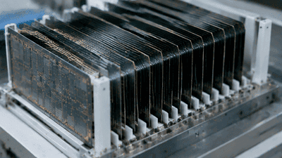
Glass core substrates replace the organic core layer with a thin glass panel onto which redistribution layers, vias, and copper wiring are built. Glass, as a core material, brings a different set of physical properties to the table:
- Excellent flatness. Glass maintains very high planarity across large areas, which is crucial for large packages with fine-pitch bumps.
- Low CTE and good matching to silicon. Glass expands less with temperature and can be engineered to closely match silicon’s thermal expansion, reducing stress and warpage.
- Finer routing potential. With better dimensional stability and smoother surfaces, glass supports tighter line/space and more precise via formation.
- Attractive dielectric properties. Low-loss glass formulations can support higher frequencies with reduced signal degradation.
In many ways, glass cores act like a bridge between silicon interposers and organic substrates: they borrow some mechanical and electrical advantages from silicon while aiming to maintain a cost structure that can be scaled more like an organic-based panel.
Glass vs. Organic: Key Technical Trade-offs
To understand the revolution underway, it is helpful to walk through the key technical trade-offs between glass core and organic substrate approaches.
1. Dimensional Stability and Flatness
Glass has an inherent advantage in flatness and dimensional stability. Large glass panels maintain planarity during processing and operation far better than organic materials, which can warp due to internal stresses, moisture absorption, and CTE mismatch.
For advanced packaging, this means:
- More reliable assembly of very large multi-die packages.
- Better yield when bonding dies at fine pitch, since warpage leads to open or shorted connections.
- Improved alignment in 2.5D/3D stacks and multi-chip modules.
Organic substrates can be engineered and designed to mitigate warpage, but glass starts with physical properties that make the problem easier.
2. Routing Density and Line/Space
As chiplet architectures proliferate, the substrate must support more signals per unit area. Glass surfaces lend themselves to fine patterning, enabling narrower lines and smaller spacing between traces under better control. Combined with advanced via drilling techniques, this can provide higher routing density than most organic cores can reliably deliver.
In heterogeneous integration, where multiple dies and memory stacks sit on a single substrate, this extra routing density can be the difference between:
- Needing an intermediate silicon interposer, with added cost and thickness.
- Routing everything directly through the glass core substrate itself.
Organic substrates are improving, but glass has a cleaner path to the ultra-fine pitches that future chiplet interfaces and high-speed networks demand.
3. Power Delivery and Signal Integrity
High-performance systems are hungry for both clean power and clean signals. Glass cores can offer low dielectric loss and tightly controlled impedance, which helps maintain signal integrity at very high data rates. Their stability also allows precise alignment of power and ground planes, reducing noise and improving power delivery network design.
Organic substrates can also achieve sophisticated power and signal structures, but the combination of material variability, warpage, and loss can be harder to tame at extreme frequencies. For AI accelerators and advanced networking chips, that difference shows up in eye diagrams, jitter, and the maximum achievable data rate without resorting to expensive mitigation techniques.
4. Thermal and Mechanical Behavior
CTE matching matters a lot when bonding large silicon dies to a substrate. Glass cores can be engineered to have a CTE that closely matches silicon, reducing thermal stress during power cycling. This reduces the risk of micro-cracks, solder fatigue, and long-term reliability issues at the die-substrate interface.
Organic substrates typically have higher CTEs, so they expand and contract more than silicon. Designers manage this through underfill materials, mechanical design, and careful package architecture, but the stress is intrinsically higher. For enormous AI packages where multiple large dies sit on one substrate, that stress becomes a prominent reliability concern.
On the flip side, glass is more brittle than organic materials. Handling thin glass panels requires careful tool design and process control to avoid cracking or chipping, especially at the panel edges. This introduces a different flavor of mechanical challenge that the industry has to solve.
Heterogeneous Integration on Glass vs. Organic
Heterogeneous integration is the art of combining different dies – logic, memory, analog, RF, sensors, power – into one advanced package. The choice of substrate influences how flexible and scalable that integration can be.
On organic substrates, heterogeneous integration tends to lean on:
- Silicon interposers for ultra-dense routing between logic and memory.
- Fan-out redistribution layers to cluster smaller dies without adding a full interposer.
- Moderately dense substrate routing to handle chiplets and peripheral dies.
On glass core substrates, designers envision:
- Using the glass core itself as a high-density interconnect fabric for multiple dies.
- Reducing reliance on separate interposers in some architectures, potentially saving cost and thickness.
- Building large, highly integrated “substrate-level systems” where chiplets are spread across a glass panel like tiles on a floor.
This does not mean glass replaces silicon interposers everywhere, but it does blur the boundary between the interposer and the substrate. In some advanced designs, the glass core may take on roles traditionally reserved for silicon, especially where ultra-large form factors or specific routing patterns are needed.
Cost and Manufacturing Considerations
Technical advantages do not automatically win the market – cost and manufacturability always have a say. Here, organic and glass cores differ in ways that will shape how fast and where each is adopted.
Organic Substrates: Economies of Scale
Organic substrates benefit from huge economies of scale. The infrastructure, tooling, and process flows are widely available, and many fabs are optimized to produce high volumes with predictable yields. For mainstream devices, that translates into:
- Lower cost per substrate at comparable sizes and layer counts.
- More options for sourcing and second-sourcing.
- Shorter lead times and more flexible capacity planning.
Even as advanced packaging pushes organic technology to its limits, cost pressures in consumer markets and mid-range servers make organic substrates the default choice unless their limitations are truly blocking the desired design.
Glass Cores: Investment and Learning Curve
Glass core substrates are still on a steeper part of the learning curve. They require:
- New handling equipment for thin glass panels.
- Refined drilling, via formation, and metallization techniques suited to glass.
- Process development to ensure high yield and robust reliability.
Initially, this makes glass cores more expensive per unit than equivalent organic counterparts. However, glass is compatible with panel-level processing techniques that promise better material utilization and high throughput once the technology matures. Over time, with proper investment, glass core substrates could achieve a competitive cost structure, especially for large, high-value packages where organic substrates are already nearing their cost and performance limits.
In other words, glass starts as a premium option for high-end, performance-driven products, with potential to move downstream as processes mature and volumes increase.
Where Each Substrate Shines
Rather than a simple winner-takes-all outcome, the advanced packaging revolution is more likely to produce a substrate landscape where glass and organic each have sweet spots.
Organic substrates are likely to remain dominant in:
- High-volume consumer devices where cost is paramount.
- Moderately complex chiplet or multi-die packages that do not need extreme panel sizes or line/space.
- Legacy and mid-performance markets where existing designs and infrastructure are entrenched.
Glass core substrates are poised to shine in:
- Large AI accelerators and HPC packages where size, flatness, and high-speed routing are critical.
- Advanced 2.5D/3D systems that combine many chiplets and memory stacks on a common substrate.
- Next-generation networking and data center devices that push signal integrity and power delivery to the edge.
As more real products adopt glass cores, design teams will gain confidence and explore architectures that simply were not practical before. At the same time, organic substrate technologies will not stand still; they will continue to improve and defend their territory with incremental enhancements and cost advantages.
Design and Co-Optimization in the New Era
One of the most important side effects of the glass vs. organic debate is the growing recognition that chip, package, and board can no longer be designed independently. Co-optimization is becoming a necessity:
- Chip architects must understand substrate capabilities early, including line/space, via density, and power delivery constraints.
- Package designers must collaborate with system teams to align thermal and mechanical strategies with rack- or device-level cooling and mounting schemes.
- Material and process engineers must feed realistic constraints and opportunities back into design flows.
Whether the substrate is glass or organic, the best designs will be those that treat it as a core part of the system, not as a fixed background. In that sense, the “advanced packaging revolution” is as much about changing mindsets and workflows as it is about switching materials.
The Road Ahead: Convergence and Hybrid Approaches
As with many technology transitions, the future is likely to be more hybrid than binary. We may see:
- Packages that combine glass cores with organic outer layers to balance performance and cost.
- Panel-level manufacturing that uses both glass and advanced organic materials, each optimized for different product tiers.
- Standardized chiplet interfaces that can be routed effectively on either substrate type, giving system designers more flexibility.
In parallel, new demands – such as co-packaged optics, integrated power delivery, and tighter 3D stacking – will continue to stress substrate technologies and push them forward. Glass may play an especially interesting role in photonics and high-speed optical interconnects, given its optical transparency and stability, though those applications are still emerging in mainstream packaging discussions.
Conclusion: A Substrate-Level Revolution
The revolution in advanced packaging and heterogeneous integration is happening surprisingly deep in the stack, at the level of the substrate that supports and connects the silicon. The debate between glass core substrate and organic substrate is not just academic; it is about who can deliver the next wave of performance, bandwidth, and integration density in a world where traditional scaling is slowing.
Organic substrates, with their maturity and cost-effectiveness, will continue to carry a huge portion of the industry. Glass core substrates, with their flatness, stability, and routing potential, are emerging as a powerful option for the most demanding systems. Together, they are redefining what a “package” can do, enabling heterogeneous integration architectures that blur the boundaries between chips, modules, and systems. In that sense, the advanced packaging revolution is not just about adopting a new material; it is about recognizing that the true platform for the next era of computing may not be a single die, but the substrate that brings everything together.





